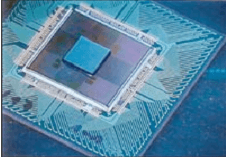
NQW has developing a structured quartz wafer (150μm + /-10 microns) and transfer into production, for a well-known customer, successful completed.
A special geometry (TTV < 10 microns), size of the holes (2.0 mm +/- 0.05 mm), the surface roughness (Ra < 0.3 nm) and the dimensions (100x100mm +/- 0.1) of the wafer presented a new challenge of our production capability.
The so-called structured spacer wafer of quartz material be used in the area of the image sensors. By the knowledge which kind of customer requirement are relevant, the development time and the introduction as a standard product has shortened. The customer was impressed with our performance and capabilities!