Glass Wafer
Wafers made of glass, are the basis of the modern micro system technology. It is especially used in the semiconductor industries. A common application is the the mechanical stabilization of thin Si-diaphragms or sensors, and etching structuring masks for MEMSs.
The glass wafer substrates are the basic components of LCD panels and OLED substrates, and the wafer quality influences the production yield. NQW materials from the major manufacturers in all grades and specifications. All glass material offered by NQW is certified by the manufacturers.
Key facts about our Production Capabilities
Glass Material
- Schott: Borofloatt33, MEMPax, AF32, AF37, B270, N-BK7, Optical Glass
- Corning: ULE Glass, Eagle XG, Optical Glass
- Other customed
Wafer Application
This material is widely used in semiconductor, medical science, communications, lasers, infrared, electronics, measuring instruments, military, and aerospace.
Dimension & Thickness
- Round Wafer 5mm up to 400mm
- Square Wafer 4x4mm up to 1000x500mm
- Thickness 100µm up to 10000µm
- TTV <10µm (Standard) up to <5µm (Premium)
- BOW +/-40µm , WARP <40µm
- Semi Flat(s), Notch or without cutoffs
- Edge: C-Shape, beveled, As Cut
Surface & Quality
- Surface Finish: Single / Double Side Polished, Lapped, Grinded
- S/D-Quality 60/40 (Standard) up to 10/5 (Premium),
- Polished Ra<1nm (Standard) up to <0,5nm (CMP)
- Lapped Ra 0,1µm up to 2,0µm
- High Contrast Lasermark with different colors
Product Examples
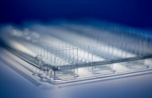
25x25mm Glass Wafer
This product is mostly used for monitoring coating processes. We can manufacture this 25x25mm substrates from different materials like Borofloat33, AF37 or D263 and in different thicknesses from 0.55, 0.7 or 1.1 mm (based on the selected material). If you’re looking for an inexpensive solution, the “As-Cut” edge quality would be the perfect choice for you.
The wafers are shipped in our custom-made trays, that can hold up 100 Substrates at once. So Storage and Withdrawal are very easy. Our production capacity is currently 80k+ wafers/year.
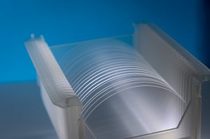
125mm Borofloat33 Wafers
Do you need a Glass Wafer for your MEMS Application? Our premium polishing process with a surface roughness (Ra) below 0,5 nm and Schott’s high quality Borofloat33 Glass Material are the best combination for your Si-Wafer bonding process. The grinded c-shape edge can be manufactured with a tolerance of +/-0.1 mm and is the budget friendly version of the T/3 or T/4 SEMI-Profile.
We established a high volume production line with a capacity of 10k+ wafer/year since 2016. For shipping we use common Boxes like Entegris Ultrapak.
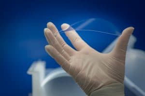
100 µm thin Glass-Wafer
We can manufacture thin flexible Glass Wafer in Standard (75, 100, 125 mm) or non-Standard (e.g. 160 mm) sizes based on your requirements. Using state-of-the-art Grinding and Polishing Processes we can achieve the same quality as on thicker Wafers.
Due to the less mechanical stability we can’t use Standard Shipping Boxes with Slots. We normally packed these thin wafer in “Coin Roils”-Type Packages with Clean Room Paper as Spacers.
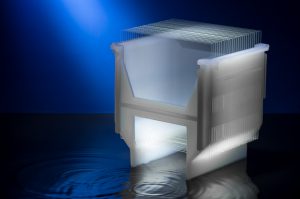
150x150mm AF37 Substrates
OLED Elements have already entered the mainstream electronic consumer products. Since 2012 we offer inexpensive substrates and services for innovative OLED manufacturers.
We are separating big Glass Sheets in smaller 150x150mm Substrates and perform a slight Edge Grinding to avoid Edge Chips during Tool and Process Handling. Based on the non-Standard SEMI-Format we shipped the Wafer in customizable packages with clean room wipes. We also produce smaller Substrates for additional inline Monitoring of the Coating Processes. Our Production Capacity is currently 4k+ Wafers/Year.
Do you need further information or a quotation?
Please feel free to call use by phone +49 (0) 9101 / 90 220 – 200 or simply use our request form.