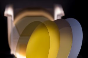
LT & LN Wafer
The basic principle of SAW devices is the generation of elastic surface waves from electrical signals and their reconversion. The substrate material is a piezoelectric crystal such quartz (SiO2), lithium tantalate (LiTaO3) or lithium niobate (LiNbO3). This are single crystal materials, which are cut out after the growth process with a defined orientation to a wafer. NQW produced this wafer for SAW manufacture and R&D centres. Please find below typical specification requirements.
LT /LN Material
- LT Lithium Tantalate (LiTaO3), LN Lithium Niobate (LiNbO3)
- LT: typical cutting X112°Y/36°Y/42°Y/48°Y/ Z-cut
- LN: typical cutting 128°Y/64°Y /41°Y /Y / Z-cut
- SAW/Optical Grade, LN Black (Free of Pyro-Electric Effect)
- MgO doped LN Wafer
Wafer Application
- SAW devices are especially used in mobile phones as dielectric filters band-pass filter, RF filter and IF filter
- broadband filters include radar technology
- remote controls for home electronics
Dimension & Thickness
- Round Wafer 4″ up to 8″
- Square Wafer 10x10mm up to 100x100mm
- Thickness 250µm, 350µm, 500µm, 1000µm
- Semi Flat(s), Edge C-Shape
- TTV <10µm (Standard) up to <5µm (Premium?)
- BOW +/-40µm , WARP <40µm
Surface & Quality
- Surface Finish: Single / Double Side Polished, Lapped, Grinded
- LTV≤0.4um EE 3mm, Within area of 5x5mm, Valid for PLTV >98% of working area
- Polished Ra<1nm (Standard) up to <0,5nm (CMP)
- Lapped Ra 0,1µm up to 0,5µm
Do you need further information or a quotation?
Please feel free to call use by phone +49 (0) 9101 / 90 220 – 200 or simply use our request form.