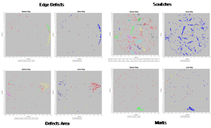
Nano Quarz Wafer has developed a system, which identifies very precisely defects, e.g. scratches, marks or faults on the edge, on quartz, glass and sapphire wafers. The automated cluster analysis and macro inspection is based on DBSCAN – Density-Based Spatial Clustering of Applications with Noise and enables Nano Quarz Wafer to analyze each wafer very carefully and ensure its quality on very high levels. The innovative system has many advantages for the industry. First of all there is no knowledge necessary regarding the number of clusters or the domains. Secondly, the method is optimized for scanning scratches and edge defects especially on quartz and glass substrates and can be dynamically adjusted to the area and to the form of the scan area. Thus, it improves the production process as well as the rework efficiency and offers an advanced process control. The new system also allows Nano Quarz Wafer to automatically compare specific criteria on the base of customer requests.
How does the defect identifying system work? It starts off by capturing the data of the image and then goes over to a real time analysis on the base of an algorithm. As a result, the system subsumes all detected defects of the wafers and shows them on error patterns. Hence the wafers can be classified. Finally the system provides a quantitative analysis of the results and a suggestion on how to proceed further.