Reclaim & Processing Service
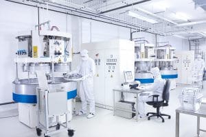
NQW is the specialist of ultra-precision processing and reclaim service for re-use of Quartz & Glass Wafer, SiC Wafer and SAW Wafer.
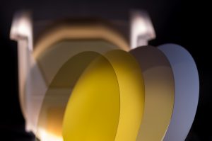
Material
- Fused Silica Wafer
- SiC Wafer
- Silicon Wafer
- Glass Wafer e.g. Borofloat33
- SAW Wafer: Quartz Crystal, LT (LiTaO3), LN (LiNO3)
Typical Reclaim (2″ – 300mm) for different materials
- Polyimid Film Removal of Glass Wafer
- Reclaim Process for LT & LN Wafer
- Fused Silica Lasermark Removal
Process steps and capabilities:
- Frontside and backside grinding down to 100µm
- Downsizing quartz and glass Wafer
- Grinding double or single side
- Lapping double or single side
- Lasermarking
- CNC – edge polishing and grinding
- customer specific glass/ quartz Wafer structures
- customer specific glass/ quartz Wafer coating
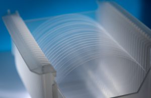
Typical Processing Services (2″ – 300mm)
- Single & Double Side Polishing service
- Wafer Cleaning Service (e.g. Handling, Teaching Wafer)
- Etching Service
- Backside Roughness (improved coating adhesion, front/backside distinction, higher contrast for laser marking)
Application Examples for NQW Services
Polyimid Film removal on Glass Substrates
We provide a reclaim process for Glass wafer with multi-layer, structured Polyimid (PI) Films. The process is based on an organic alkaline chemical solutions and an additional mechanical cleaning / polishing to remove the Polyimid Film from the surface of the glass wafer. The reclaimed glass wafers can be returned to the customer production process with no or a minimal loss on thickness. The customer used PI Technology with glass wafer for flexible integrated circuits (FlexICs).
Refurbish of Coated LT/LN Wafer
NQW provide a etching and chemical mechanical polishing process for structure wafer of Lithium tantalate and Lithium nobiate wafer.
Surface Lapping to improve Coating Adhesion
We have various micro-inch lapping procedures to achieve superior results for Coating Adhesion at surfaces. This experience, applied to your problems, ensures the highest quality geometric and dimensional accuracy.
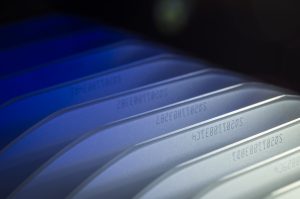
Lasermarking on lapped or blank substrates
The unique marking on wafers is for tracking and tracing in complex manufacturing processes essential. For Research and Development (R&D) a direct identification of a substrate is also helpful to track the process history and results.
We can produce laser marks on various substrates with low stress, so there is no risk for breakage or cracks. The marking itself with letters, fonts, codes or content can be flexibly adapted to your needs. To achieve a good visibility on clear substrates we can apply a lapped surface on the complete wafer or only on defined local areas.
Do you need further information or a quotation?
Please feel free to call use by phone +49 (0) 9101 / 90 220 – 200 or simply use our request form.